Introduction to STEM
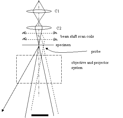
Some TEMs have scan coils which allow them to be used as a
scanning transmission electron microscope (STEM). In STEM,
a conical electron beam is focussed through the specimen by
a lens in front of the specimen (C2 and the objective lens
pre-field), as shown below.

The optical configuration is roughly the same as simply
forming an image of the filament by focussing C2 – the very
first experiment we did in the electron microscope. In
fact, if your microscope has a twin objective lens, the
optics are a little bit more complicated, but lets start
thinking about things as simply as possible.
The tight beam cross-over at the specimen plane is usually
called an electron ‘probe’. Images can be formed by
scanning the probe across the specimen (by the double-
deflection shift coils) and detecting the transmitted
electrons, which are either on the optic axis (to form a
bright-field image) or have been scattered to high angles,
to form a dark-field image.
In order to make an image, we have to display the signal
coming out of one or more detectors in some way. This is
usually done on a slow-scan television screen (although it
is nowadays also done by computer). The signal detected is
used to modulate the intensity of the image on the display
screen, while the scan of the display is synchronised
accurately with the position of the probe on the specimen.
Usually, the same ‘scan generator’ is used to control both
the x-y position of the beam (or probe) shift deflection
coils and the coils that control the display screen. The
principle is the same as a conventional scanning electron
microscope.
A STEM doesn’t actually need any lenses below the specimen
at all, because everything important happens before the
electrons reach the sample. In practice, a TEM/STEM has all
the usual objective lens and projector lenses below the
sample (shown as a dotted box above), but in STEM
mode these are just used to change the effective camera
length between the specimen and the detector plane. They
can also be used to form an image of the electron probe.
Although there are certain benefits of STEM imaging (which
have not been generally been recognised until quite
recently), the main advantage of this geometry is the fact
that the probe can be used to irradiate a very small volume
of specimen in order to obtain all sorts of other signals
such as characteristic X-rays, Auger or secondary electrons,
or electron energy-loss spectra. All these signals can be
spatially resolved at a resolution corresponding to the
width of the probe, thus allowing for high resolution micro-
analysis. For the material scientist, analytical signals
like these can be much more useful than simply images, say
to identify the elements present in an inhomogeneous sample.


Copyright J M Rodenburg
| 
